Today's topic is on graphene and it's crystal lattice. Semiconductors are "grown" in these lattices using expensive equipment.
Carbon, in particular, grows in many different forms, from diamonds to pencil lead (yes, you can even make diamonds in a lab). Graphite is used in pencil lead because its layers detaches from the lattice easily, making it ideal for writing.
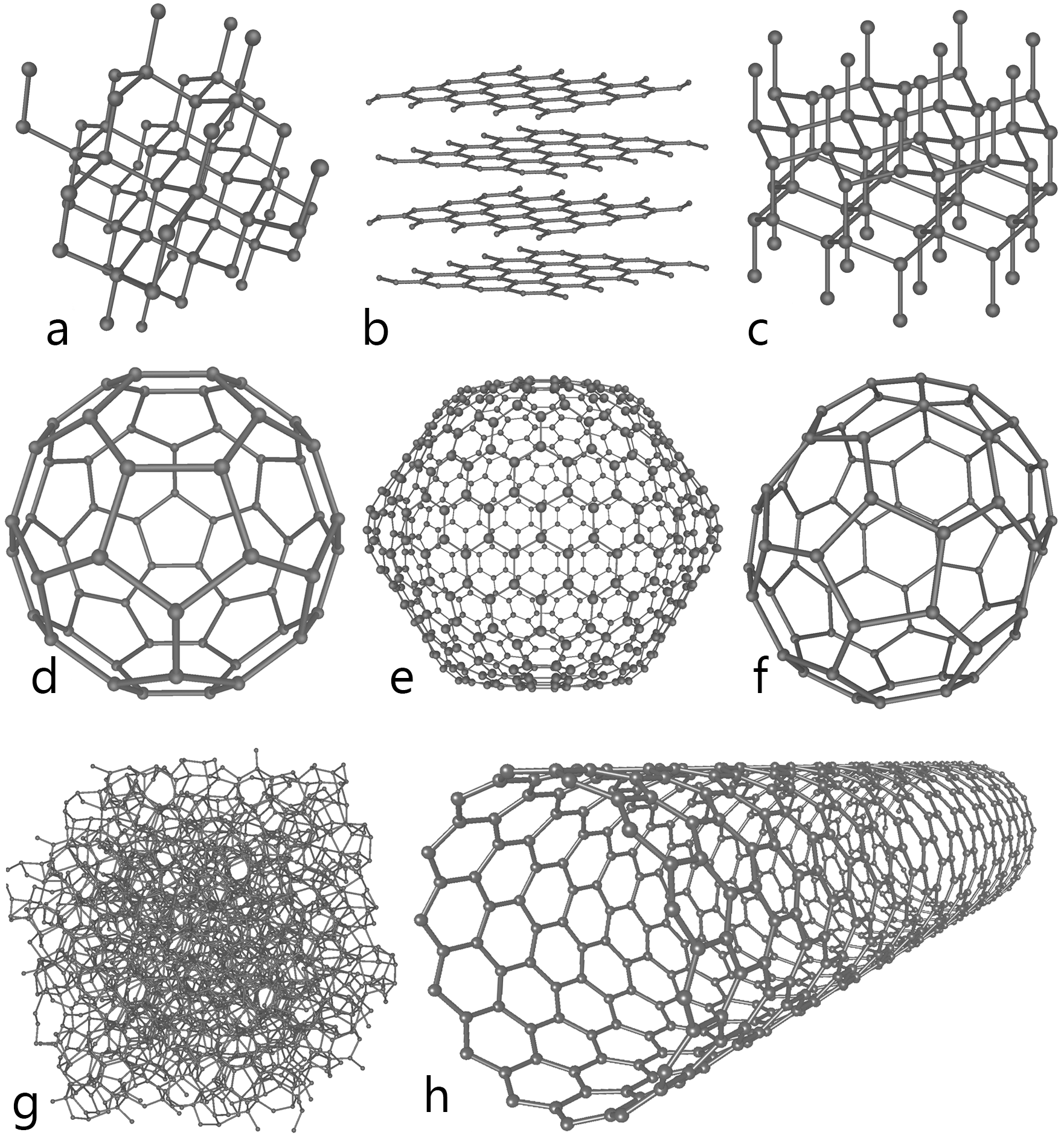
In the above picture, "b" shows sheets of graphene, which when stacked on top of each other makes graphite The diagram entry of "h" shows a carbon nanotube, which is a sheet of graphene rolled into a tube.
Two researchers named Andre Geim and Konstantin Novoselov discovered graphene, a single sheet of graphite (and subsequently received the Nobel Prize in Physics 2010 for it). This single atom thick sheet can have an enormous amount of applications as we continue to shrink the size of our electronic devices. In graphene, electrons have a very high mobility, and they can move very fast, making it ideal for high speed circuitry. Also, a single layer of carbon is relatively easy to see through, opening up new possibilities for digital display screen technologies.
Here's a link detailing the two researchers Nobel Prize:
http://nobelprize.org/nobel_prizes/physics/laureates/2010/#
Yeah I've heard that you need something as big as an elephant to break a pencil sized graphene!
ReplyDelete